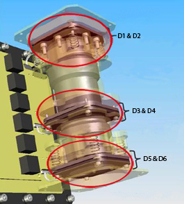
CRaTER Solid State Detectors
Solid state detectors use semiconducting crystals (in CRaTER's case, silicon) with n-type (electron-rich, electron conducting) and p-type (electron-deficient, hole conducting) sectors.
 |
|---|
Pairs of thick and thin silicon detectors (highlighted in red) |
When a reversed bias voltage is applied at the p-type side, the unbonded electrons in the semiconductor are pushed away from the voltage source, while the holes are pulled towards it. This leaves a neutral area void of charge and current at the junction of the sectors, called the depletion region.
As incoming ionizing radiation (glactic cosmic rays or solar protons) collides with the depletion region, electron-hole pairs are formed in the material (where a once bonded electron is freed from its atom, leaving a hole). The electron and the hole respond to the applied voltage, and a small current is created. This current can be detected and later analyzed.

